Press release
Imec advances Europe's silicon interposer technology capabilities through NanoIC pilot line, paving the way for open chiplet design
Baseline flows of NanoIC’s silicon interposer platform mark key step towards open-access PDKs, helping organizations better explore and prepare for next-generation chiplet-based systems.
LEUVEN (Belgium), NOVEMBER 10, 2026 — This week at SEMICON Europa 2026, imec announced that it delivered the baseline flows for the silicon interposer platform being developed within the NanoIC pilot line.Providing an early technical view of a key technology for chiplet integration, the milestone represents an important step toward more accessible advanced packaging innovation in Europe.
The silicon interposer is one of three advanced interconnect technologies being developed within NanoIC, alongside fine-pitch RDL interposers and die-to-wafer hybrid bonding. Together, these technologies are being translated into dedicated process design kits (PDKs) and, ultimately, future low-volume prototyping opportunities, helping organizations better explore and prepare for next-generation chiplet-based systems.
Opening access to silicon interposer technology
As the performance requirements of advanced compute for AI continue to rise, the semiconductor industry is increasingly turning to chiplet architectures which combine multiple specialized dies within a single package. Their performance, however, depends not only on the individual chiplets, but also on the connections between them.
Advanced packaging and interconnect technologies have therefore become a critical area of innovation, enabling higher bandwidth, lower energy consumption, and tighter system integration.
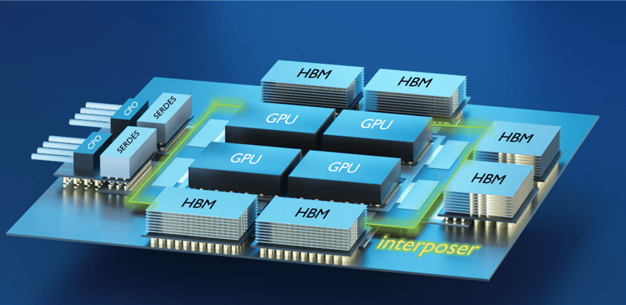
Silicon interposers are a critical enabler of this transition. Acting as a high-density routing layer beneath the dies, they provide the short, dense connections needed to link compute chiplets, high-bandwidth memory and other specialized components. This makes them particularly relevant to AI accelerators, GPUs and other high-performance multi-die systems, where bandwidth and energy-efficient data movement are decisive system-level requirements.
Building on this need for high-density chiplet connectivity, imec is now establishing a technical reference platform for its silicon interposer technology within the NanoIC pilot line, helping organizations explore the technology and its potential for advanced chiplet integration.
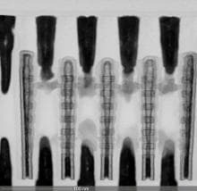
The platform captures the architecture, manufacturing flow, and key design characteristics of imec's silicon interposer technology. This includes features such as through-silicon vias, multiple metal routing layers and support for microbump pitches down to 20 µm, enabling the high-density connectivity required between chiplets, memory and other specialized dies within a single 2.5D package.
From a technology reference to a design-ready PDK and tape-out opportunities
The baseline flow underpinning this technical reference platform functions as the technical basis for a dedicated silicon interposer process design kit (PDK), scheduled for release early 2027. This PDK will allow universities, start-ups, and fabless companies to virtually explore silicon interposer technology, using industry-standard EDA environments as provided by Cadence and Synopsys.
In doing so, it will help build expertise in the possibilities of advanced packaging and prepare for next-generation heterogeneous systems before the technology is introduced into manufacturing.
When launched, the silicon interposer PDK will complement NanoIC's already available interconnect PDKs for fine-pitch RDL interposers and die-to-wafer hybrid bonding. “Together, these technologies address different aspects of advanced chiplet integration. Silicon interposers enable the high-density routing required for advanced compute applications, fine-pitch RDL interposers offer a cost-efficient alternative for integrating chiplets at high interconnect densities, while die-to-wafer hybrid bonding enables ultra-dense chip-to-chip connections. By making these three complementary technologies available through dedicated PDKs, NanoIC gives designers a unique toolbox to explore and evaluate their system architectures,” Marie Garcia Bardon, department director at imec and work package leader within the NanoIC project, explains.
Looking ahead, NanoIC's longer-term ambition is to extend this virtual exploration via a PDK into physical silicon demonstrators on the pilot line.
This is particularly important in a rapidly evolving landscape. “With the rapid evolution of AI, it is becoming harder to predict which combination of compute, memory and accelerator technologies will deliver the best performance for a given application. Chiplet-based integration allows system designers to combine different compute, memory and accelerator technologies within a single package and adapt those combinations as requirements evolve. But that approach can only succeed if the chiplets can exchange data quickly and efficiently. By providing a common technology foundation for advanced interconnect technologies and making them accessible through advanced PDKs, NanoIC enables researchers, start-ups and fabless companies to experiment with the different interconnect approaches, evaluate future system architectures and build expertise in advanced packaging. In doing so, it helps Europe, and its strategic European markets, prepare for the next generation of physical AI, automotive and advanced computing systems," Bart Placklé, senior vice president of automotive technologies at imec, summarizes.
This work has been enabled in part by the NanoIC pilot line. The acquisition and operation are jointly funded by the Chips Joint Undertaking, through the European Union’s Digital Europe (101183266) and Horizon Europe programs (101183277), as well as by the participating states Belgium (Flanders), France, Germany, Finland, Ireland and Romania.
Want to take a closer look at the technology behind NanoIC’s silicon interposer platform?
Explore the technical reference document for more details on the platform architecture, key design features and process flow.
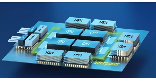
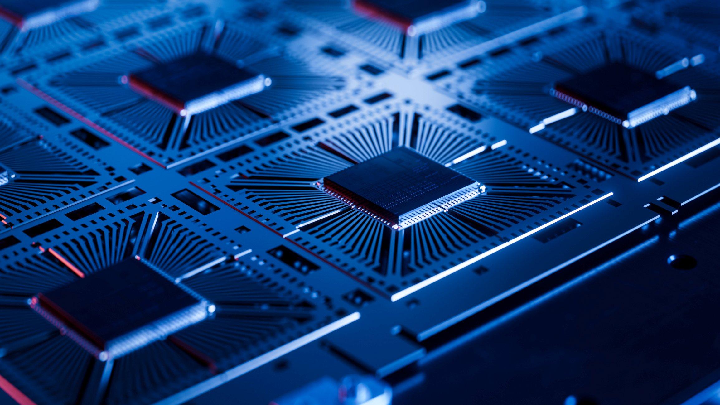
Conceptual representation of NanoIC's silicon interposer on a chip.