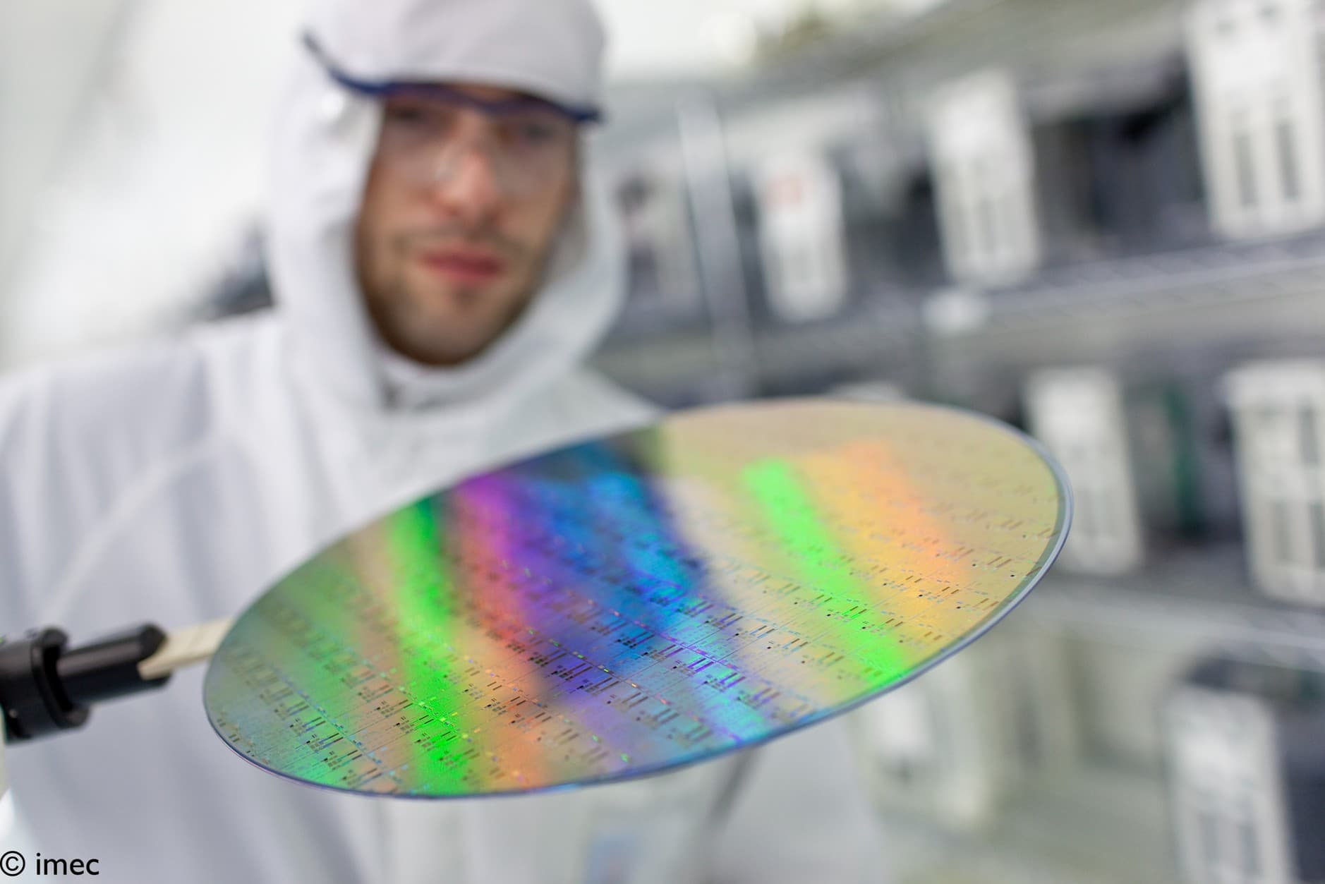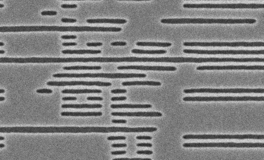

The Swedish semiconductor equipment company AlixLabs has launched a six-month evaluation project to assess the potential of its APS™ technology for advanced semiconductor patterning within the NanoIC pilot line, coordinated by imec.
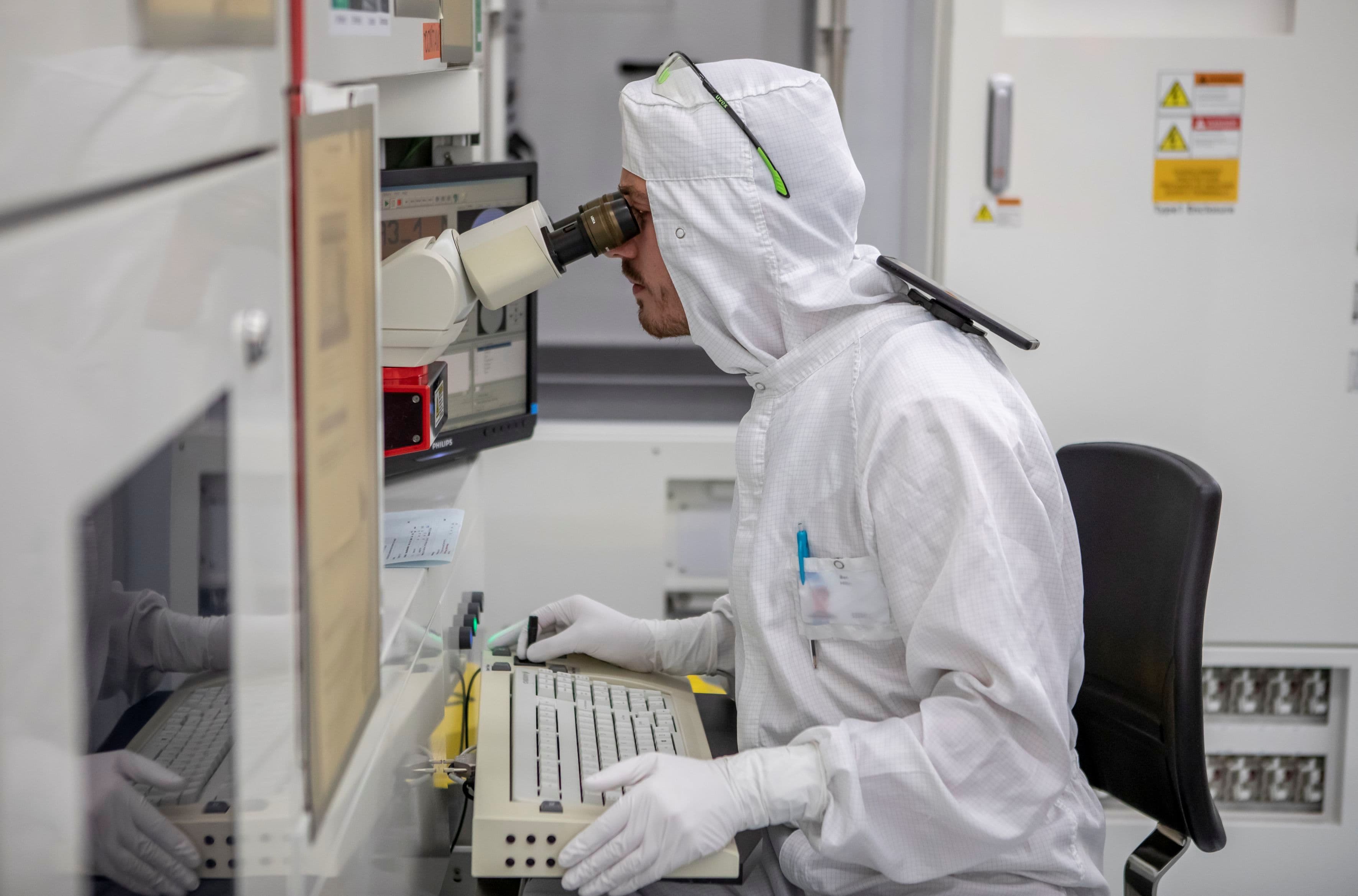
The project combines AlixLabs’ atomic layer etch-based pitch splitting process with imec’s advanced lithography, process integration and metrology capabilities, made available through the infrastructure of the NanoIC pilot line.
“This evaluation gives AlixLabs the opportunity to assess APSTM in a highly relevant and rigorous semiconductor pilot line environment,” Jonas Sundqvist, CEO of AlixLabs, said. “The strategic value for us is the ability to generate data using imec’s established expertise, metrology and process methodology. It is an important step in demonstrating where APSTM can contribute within advanced patterning and in advancing our role in the European semiconductor technology ecosystem.”
The collaboration also illustrates NanoIC's mission to support the maturation of innovative semiconductor technologies.
“The NanoIC Pilot Line is designed to help innovative semiconductor technologies mature in an advanced pilot manufacturing environment. Our collaboration with AlixLabs combines its APS™ technology with imec’s expertise in lithography, process integration, and metrology to assess the potential of a novel patterning approach using industry-relevant metrics. This project highlights the value of ecosystem collaboration in accelerating innovation, reducing development risk, and strengthening Europe’s semiconductor technology leadership,” said Giuseppe Fiorentino, program manager at imec.
Want to learn more about the collaboration and methodology?