
The semiconductor industry is evolving at breathtaking speed. From intensive AI workloads in agentic and physical AI to real time decision making in autonomous systems such as self driving vehicles or smart sensing platforms, the demand for high-performance compute continues to grow exponentially, turning compute scalability into one of the defining challenges for the semiconductor ecosystem.
For many years, this rising demand for advanced compute was largely met through transistor scaling, with predictable gains in performance, power efficiency and cost, every time a new node was reached.
Today, the bottleneck has shifted beyond compute itself: memory bandwidth and latency, the energy cost of data movement, and the efficiency of interconnects between compute, memory and chiplets have equally become decisive factors, making chip design vastly more complex.
To navigate this growing design complexity, and to actively support innovation in the race towards advanced compute, NanoIC developed its advanced process design kits (PDKs). Built within Europe’s NanoIC pilot line at imec, these PDKs provide early, technology-embedded access to future logic, memory, and interconnect technologies.
They allow designers and system architects to accelerate learning, explore design trade offs and shape next generation architectures well before industrial PDKs become available.
“Process design kits are essentially the handshake between technology and design. They capture the physical and electrical behavior of components manufactured in the fab and enable circuit designers to explore, compare, and build next-generation chips within a technology validated environment.”
Anita Farokhnejad, XTCO program manager at imec
Two types of PDKs addressing different stages of exploration
NanoIC distinguishes two complementary types of PDKs: pathfinding PDKs and system exploration PDKs. Each tackles a different set of challenges, from future logic exploration to system-level validation of advanced memory architectures and interconnects.
Pathfinding PDKs to explore logic nodes beyond 2nm
The design pathfinding PDKs focus on the exploration of advanced technologies beyond 2 nm, with a primary emphasis on logic nodes. Built on predictive models derived from imec’s process flows, they turn state-of-the-art logic technologies into a specific design toolkit for early power performance evaluation and architectural decision making.
“Pathfinding PDKs are about connecting today’s design work with tomorrow’s technology, offering an early, credible view of what future logic technologies could look like. In the race beyond 2 nm, you can’t tape out a real chip, because the technology isn’t broadly accessible yet, but you can design circuits virtually and explore realistic power performance scenarios long before hardware is available.”
Anita Farokhnejad, XTCO program manager at imec
For research institutes and academia in particular, these design pathfinding PDKs represent an important step forward on the learning curve. As advanced logic nodes have gradually become more complex, the higher abstraction layers used traditionally at universities gradually drifted away from the physical implementation reality, making it harder to produce designs that translate to the most advanced technologies.
By providing early access to logic nodes that extend beyond 2nm, NanoIC’s pathfinding PDKs reconnect system-level research with realistic physical design. This allows universities and research institutes to evaluate and benchmark ideas in a technology context that again reflects where the industry is going.
“Historically, universities could conduct meaningful and relevant research at higher levels of abstraction, without detailed access to the underlying technology. But with the shift to advanced semiconductor technology nodes, conducting impactful research in computing architectures without direct access to technology has become nearly impossible. As a result, academic research has gradually drifted away from the realities of industrial practice. That’s why the NanoIC pilot line is so important: by providing access to pathfinding PDKs, it bridges the gap between academia and industry.”
Mehdi Tahoori, professor & chair of Dependable Nano-Computing at the Karlsruhe Institute of Technology and scientific director at imec
When we look at the specific timeline, NanoIC’s design pathfinding roadmap foresees PDKs for the N2, A14 and A7 logic nodes, as well as for emerging memory technologies such as spin–orbit torque MRAM (SOT-MRAM).
At present, the pathfinding PDKs for N2 and A14 are already available. The A7 design pathfinding PDKs and SOT-MRAM PDKs are expected to be launched in 2027.
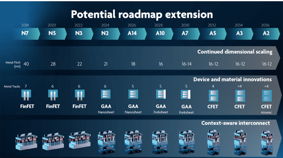
NanoIC scaling roadmap: foreseen NanoIC offerings include pathfinding pdks for N2, A14 and A7 logic nodes.
System exploration PDKs: from architectural concepts to hardware validation
While pathfinding PDKs focus on early design exploration within the scaling roadmap, system exploration PDKs are geared toward connecting architectural concepts with actual prototyping and eventually tape-out on the pilot line. In doing so, they bridge the gap between early stage research and manufacturable technology, by allowing design concepts to be evaluated within a realistic technology and integration context.
They are particularly relevant for industrial system architects, chiplet designers, startups, and applied research teams who want to prototype and evaluate how advanced technologies, such as embedded memory and interconnects, behave within realistic system architectures.
They include PDKs for eDRAM, fine-pitch redistribution layers (RDL), die-to-wafer hybrid bonding (D2W), and interposers. Together, these form key building blocks for next generation computing systems, with applications ranging from AI and high performance computing to industry driven domains such as automotive, health, and aerospace, where efficient data processing and system integration are becoming increasingly critical.
"In the race towards higher compute capacity, it will be essential to bring memory closer to the compute to reduce latency, bandwidth, and power penalties; and increase architectural flexibility by means of heterogeneous integration, chiplet partitioning, and ever more efficient interconnects. NanoIC’s system exploration PDKs are designed to explore exactly this shift. They allow designers to quantify and compare memory density and latency, interconnect bandwidth and energy, thermal constraints, and the architectural trade-offs of moving memory closer to compute."
Marie Garcia Bardon, department director & principal member of technical staff at imec
In essence, NanoIC’s system exploration PDKs allow architects to move beyond traditional, planar chip designs and go toward tape-out of complex multi-die and vertically integrated systems. By grounding these explorations in technologies that are maturing on the NanoIC pilot line, system exploration PDKs bridge the gap between emerging semiconductor technologies and future system architectures, enabling a realistic evaluation of complex system designs.
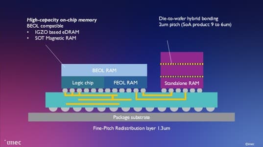
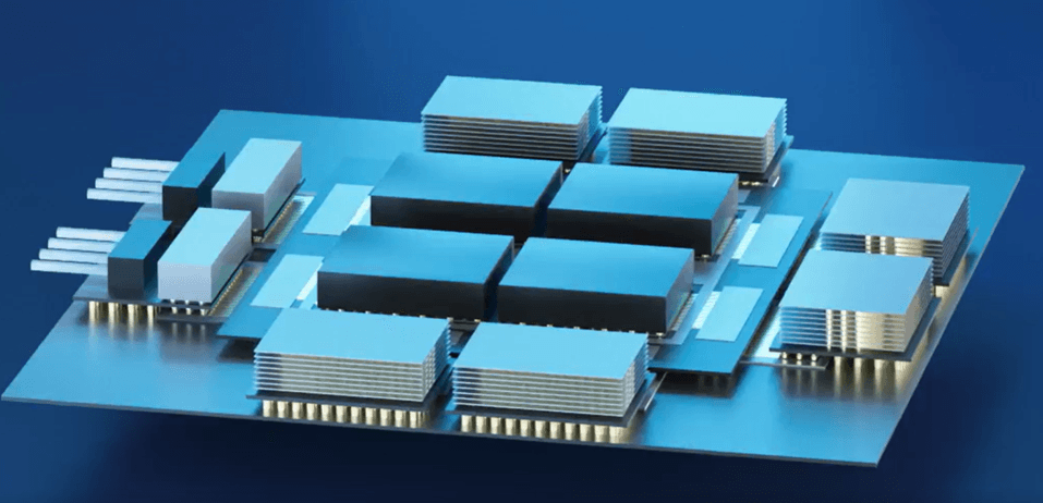
Overview of a high-performance computing (HPC) system architecture, illustrating memory placed close to compute and the use of die-to-wafer hybrid bonding and fine-pitch redistribution layers (RDL) to optimize vertical and horizontal data flows. Through NanoIC’s system exploration PDKs, architects can evaluate these integration strategies at an early stage.
NanoIC’s system exploration PDKs evolve in parallel with hardware maturity on the pilot line, progressing from architectural exploration toward real silicon demonstration and tape-out.
Today, NanoIC’s system exploration PDKs for eDRAM, fine pitch RDL and die to wafer hybrid bonding are already available. Additional PDKs, including advanced interposer solutions, will be introduced early 2027.
How the PDKs evolve over time: from v0.0 to v2.0
Unlike traditional foundry PDKs, which are typically released only at high technology maturity, NanoIC’s PDKs evolve progressively in parallel with technology readiness levels (TRLs). Successive PDK versions introduce increased functionality, improved calibration and richer design content as more process and hardware data becomes available.
Early v0.0 PDKs are close to a proof-of-concept stage, relying on process assumptions and early device data to enable functional exploration. With v1.0 releases, models are refined and calibrated across operating conditions such as voltage and temperature, supporting increasingly realistic design evaluations. v2.0 PDKs further extend this capability by enabling demonstration in context, through the introduction of statistical data sets and initial IP blocks. Later stages move toward platformization, where technologies can be more broadly reused and integrated into system-level design flows.

Overview of PDK releases following technology maturity increase.
In essence, this growing maturity can be compared to the development trajectory of a start-up. Early PDK versions primarily support learning and exploration, allowing designers to discover new concepts and validate assumptions. As the PDKs mature, they increasingly enable ideation, architectural exploration, and de-risking. In later phases, the focus shifts toward prototyping and system demonstration, as technologies approach practical implementation and tape-out on the pilot line.
Depending on the type of PDK, this progression can also take different forms across PDKs. Embedded memory and interconnect technologies, for example, typically start at a higher TRL and advance more rapidly toward hardware validation and tape out oriented use cases, whereas advanced logic PDKs remain focused on architectural design exploration rather than direct manufacturability. So the actual flow of maturation might vary per PDK.
An ecosystem approach to system innovation
That being said, one theme consistently emerges across all NanoIC PDK versions: early access is the defining value of these releases. The PDKs are designed to provide meaningful insight into future technologies at every stage of the maturation process.
By providing this unique access and turning emerging logic, memory, and interconnect technologies into usable, technology grounded design environments, NanoIC does more than support chip design, it actively lowers the threshold to European IC designers to engage with state of the art technologies.
In the race for advanced compute, these PDKs aim to enable designers and architects to move faster up the learning curve: from early stage design investigation to prototyping and, where maturity allows, tape out.
As such, by enabling predictive design environments and fostering collaboration across academia, research centers, start ups and industry across Europe, NanoIC aims to lay the foundation for a resilient European semiconductor ecosystem, one capable not only of designing tomorrow’s chips, but of sustaining the pace of innovation required to compete in the global race for compute power in the decades ahead.
Interested in getting access to NanoIC’s PDKs?
Today, NanoIC has already launched several design pathfinding and system exploration PDKs. The design pathfinding PDK offering now includes PDKs for the N2 and A14 logic nodes. System exploration PDKs are available for eDRAM, fine pitch redistribution layers (RDL) and die to wafer hybrid bonding (D2W).
Want to access these PDKs? Then go to the NanoIC PDK access page. Or register for the NanoIC mailing list to stay up-to-date of upcoming PDK releases.
This article appeared earlier in Elektronik Praxis.
This work was enabled by the NanoIC pilot line. The acquisition and operation are jointly funded by the Chips Joint Undertaking, through the European Union’s Digital Europe (101183266) and Horizon Europe programs (101183277), as well as by the participating states Belgium (Flanders), France, Germany, Finland, Ireland, and Romania. For more information, visit nanoic-project.eu.
Funded by the European Union. Views and opinions expressed are however those of the author(s) only and do not necessarily reflect those of the European Union or Chips Joint Undertaking. Neither the European Union nor the granting authority can be held responsible for them.