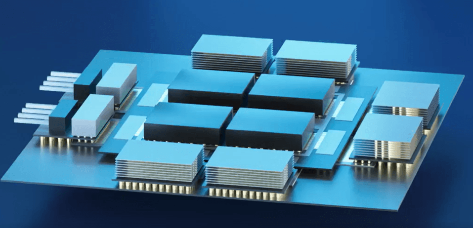
Imec recently inaugurated the NanoIC pilot line at its Leuven headquarters, marking a decisive step towards accelerating innovation in sub-2nm systems-on-chip, and reinforcing Europe at the forefront of next-gen semiconductor innovation and manufacturing.
To drive this ambition, imec focuses on the development and maturation of selected advanced logic, memory, and interconnect technologies.
For logic, efforts are centered on developing process steps, modules and baseline flows to extend the current gate-all-around (GAA) nanosheet transistor-based roadmap and develop its successor: the complementary FET (CFET).
CFET architectures, with n- and pMOS transistors stacked on top of each other, have made remarkable strides in recent years. Of all possible integration flows, monolithic CFET (mCFET) offers the fastest path to CFET introduction at industry-relevant dimensions.
However, industry may only be willing to adopt this disruptive device architecture if it can be used across successive technology nodes.
In a new design-technology co-optimization (DTCO) study, imec highlights the key performance boosters that enable mCFET scaling from A7 to A5 to A3 technology nodes.
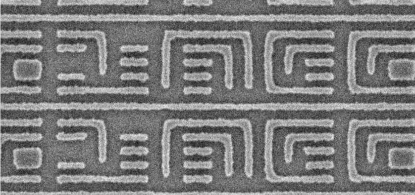
For the A3 technology node, the study identifies hybrid channel orientations for the n- and pMOS transistors as a key lever for boosting performance. Imec researchers experimentally demonstrated the key process module that makes mCFETs with hybrid channel orientations a manufacturable option.
Discover how these new insights support the NanoIC pilot line’s mission to accelerate the development of beyond-2nm logic technologies.
Published on:
27 February 2026