Press release
NanoIC extends its PDK portfolio with first A14 logic and eDRAM memory PDK
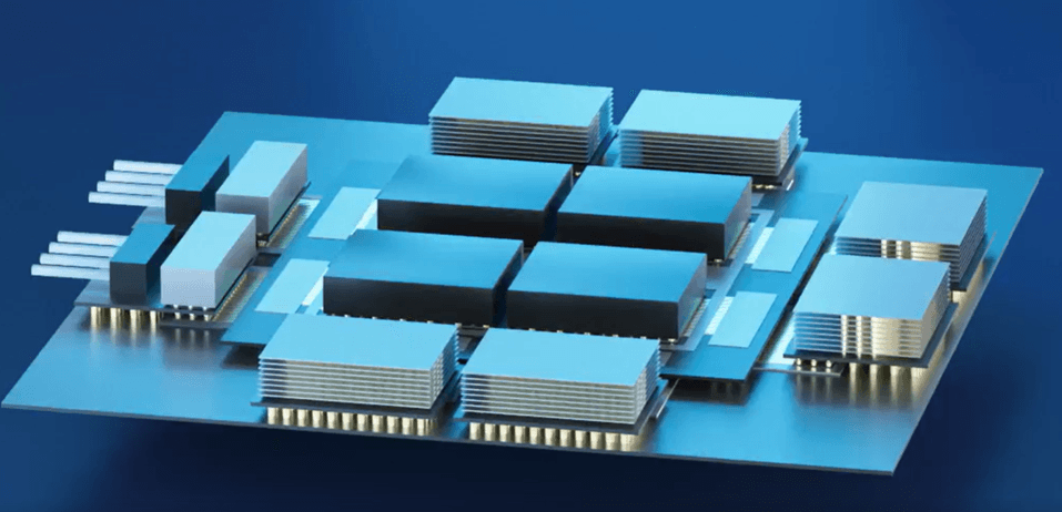
LEUVEN (Belgium), FEBRUARY 2, 2026 — Today, the NanoIC pilot line, a European initiative coordinated by imec and dedicated to accelerating innovation in chip technologies beyond 2nm, announces the release of two new process design kits (PDKs): an A14 pathfinding PDK for advanced logic scaling and an eDRAM system exploration PDK for advanced memory innovation. Both PDKs are first‑of‑their‑kind releases, providing early access to cutting-edge design rules and flows, and giving users a unique gateway to investigate advanced technology nodes and embedded memory designs.
The advanced process design kits (PDKs) from the NanoIC pilot line play a key role in advancing semiconductor innovation. They give designers early access to realistic design rules and implementation workflows long before hardware for a new technology exists. With the introduction of the A14 and eDRAM PDKs, NanoIC for the first time gives designers early insight into two critical technology areas for future compute systems: logic scaling at the A14 angstrom node and embedded memory integration.
By making these PDKs freely accessible, NanoIC seeks to connect early-stage design exploration with real-world integration, helping researchers and start‑ups explore emerging nodes, anticipate integration challenges, and benchmark designs against realistic scaling metrics. “PDKs like A14 and eDRAM are catalysts for learning and design”, Marie Garcia Bardon, department director at imec and work package leader within the NanoIC project, explains. “They offer a robust environment for hands-on evaluation and quantitative comparison of different technology choices. This approach accelerates learning, de-risks architectural and design innovation, and helps designers prepare for advanced logic nodes and embedded memory technologies well before hardware becomes available.”
“By making these PDKs broadly accessible, we lower barriers for universities, industry, and start‑ups to engage with next-generation technologies”, Giuseppe Fiorentino, program manager for NanoIC continues. “Access to realistic rules and flows enables teams to explore new research directions and breakthrough concepts that will feed directly into the European semiconductor value chain.”
A14 pathfinding PDK: scaling down to the 14-angstrom node
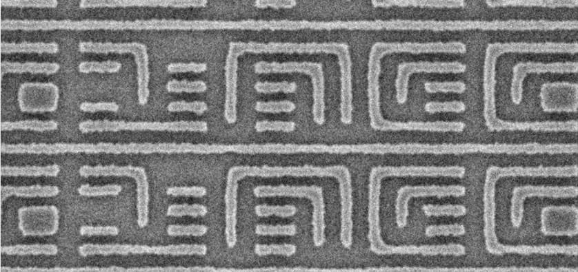
As the first of the newly launched PDKs, the A14 pathfinding PDK provides a virtual design environment for exploring scaling at the 14‑angstrom node, one of the next major steps in device miniaturization. A key innovation at this node is the introduction of a direct backside contact as a new scaling booster. Whereas the earlier N2 PDK supported backside power delivery through TSV‑Middle (TSVM) structures, the A14 node advances this concept by replacing TSVM with a more compact direct backside contact scheme. By routing power directly from the wafer’s backside to the gates and removing the need for complex top‑side metal routing, this architecture reduces IR drops and delivers an 18% area gain and 7% power reduction compared to N2 at iso frequency and cell density.
Imec is the first to release a PDK at this node. The kit includes a comprehensive 162‑SDC library and is supported by two major EDA vendors, Cadence and Synopsys.
eDRAM system exploration PDK: enabling embedded memory exploration
Complementing the logic pathfinding work enabled by the A14 PDK, the NanoIC pilot line also introduces a first eDRAM system exploration PDK, an important step toward addressing one of the biggest challenges in advanced systems: providing dense, low-latency on-chip memory. Central to this effort is bringing memory closer to the processing units, a key strategy for reducing latency and improving power efficiency in advanced compute architectures.
The current eDRAM PDK provides a virtual platform for exploring embedded memory solutions that bridge the gap between dense but power-hungry off-chip DRAM and fast but area-limited on-chip SRAM. With a focus on system‑level behavior in data‑intensive and AI workloads, it enables researchers to evaluate new memory architectures and integration strategies that bring higher‑density memory closer to processors and GPUs, reducing data movement, improving energy efficiency, and enhancing overall system performance.
Looking ahead, the eDRAM PDK will evolve into a full system exploration platform. This next phase will allow designers to move beyond virtual validation and analyze complete system-level interactions. As the platform matures, future development steps include hardware validation and, eventually, opportunities for tape‑out and prototyping on the NanoIC pilot line.
Access and training opportunities
Both PDKs, together with the previously launched N2 PDK, are available through Europractice. To encourage adoption and hands-on exploration, NanoIC will also host a dedicated workshop on the N2 and A14 PDK on March 25–26, 2026, and on the eDRAM PDK on May 26, 2026. These workshops will offer practical guidance, technical insights, and direct interaction with the development teams.
This work has been enabled in part by the NanoIC pilot line. The acquisition and operation are jointly funded by the Chips Joint Undertaking, through the European Union’s Digital Europe (101183266) and Horizon Europe programs (101183277), as well as by the participating states Belgium (Flanders), France, Germany, Finland, Ireland and Romania. For more information, visit nanoic-project.eu.
Want to get early-access to the A14 or eDRAM PDK?
Click for access
Interested in joining one of the PDK workshops to get hands-on experience with the PDKs?
Published on:
2 February 2026