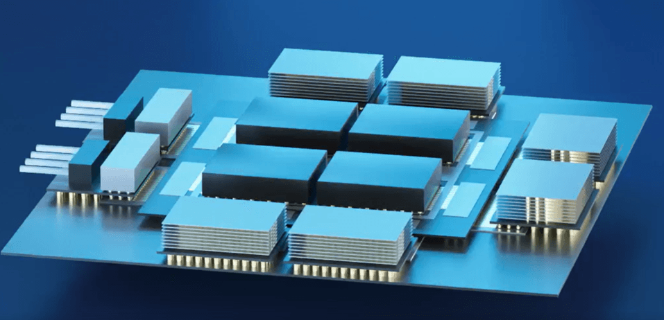
High NA EUV lithography is a critical enabler for future technologies such as advanced AI chips, high-performance computing, and next-generation memory. As such, the technology plays a critical role in realizing the European Chips Act’s ambitions for developing sub-2nm technology nodes.
But why does industry need High NA (0.55NA) EUV lithography for the next era of chip manufacturing? What are the key drivers behind the development of the world’s most advanced lithography and patterning technology?
In a detailed article, Geert Vandenberghe, VP R&D for patterning technology programs at imec, reviews the technology’s three main drivers:
- Higher resolution beyond what 0.33NA EUV can deliver.
- Process simplification and cost of technology reduction.
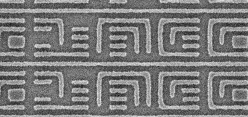
- Greater design flexibility by supporting 1.5D, 2D, and curvilinear chip layouts.
What’s more: imec and its ecosystem partners have made great strides in experimentally validating each of these promises.
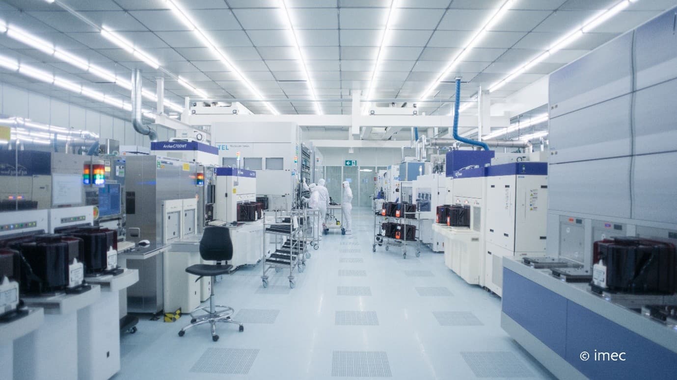
As highlighted by the author, this has been enabled through critical inflection points in the development of the litho and patterning ecosystem, i.e., materials and patterning processes, masks and imaging technology, metrology and inspection, and design techniques.
Published on:
26 February 2026