
Get early access to NanoIC’s PDKs
The NanoIC pilot line’s mission to accelerate beyond-2nm innovation relies heavily on the development and dissemination of advanced process design kits (PDKs).
These kits are crucial for both academic and industrial design communities. They not only provide hands-on experience with advanced technology nodes but also enable designers to explore emerging memory architectures and innovative interconnect technologies. By working with these PDKs, users can also deepen their understanding of cutting-edge concepts like system-technology co-optimization (STCO) and backside power delivery networks (BSPDN).
Thanks to this early access, designers – including those from fabless companies – can tackle complex challenges and explore new possibilities. It accelerates the adoption of beyond-2nm technologies and fosters innovation across the entire ecosystem.
The NanoIC pilot line offers two complementary PDKs:
- Design pathfinding PDKs: for early design exploration in beyond-state-of-the-art lC technologies.
- System exploration PDKs: preparing for hardware prototyping alongside technology development.
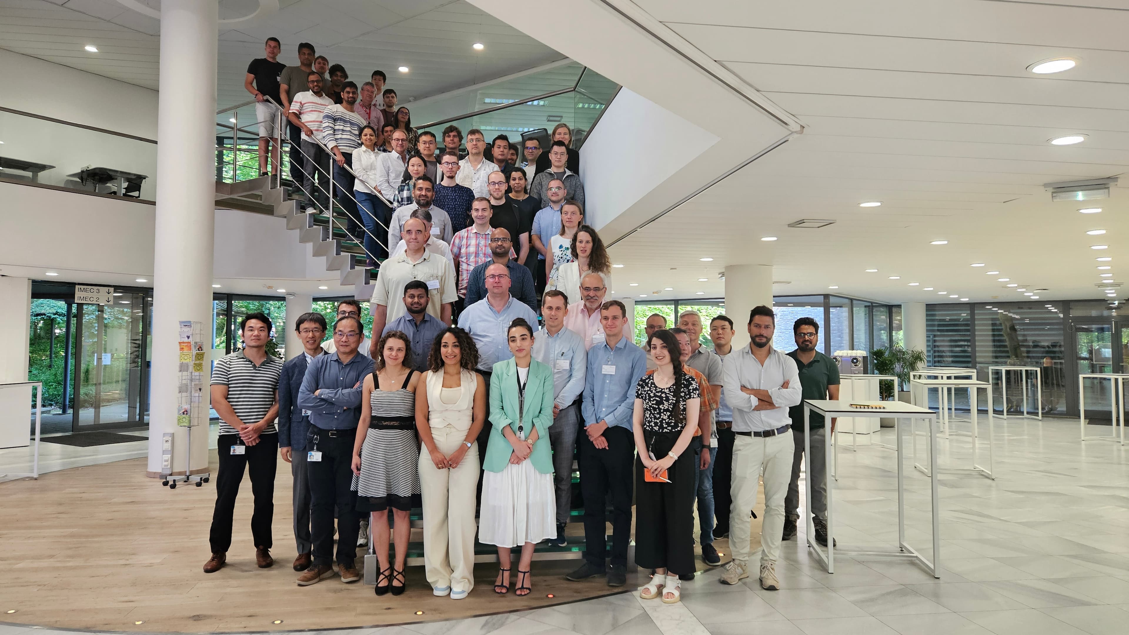
Participants of imec’s 2024 N2 P-PDK workshop, who received training in advanced-node design. Read the report.
Design pathfinding PDKs
The design pathfinding PDKs (P-PDKs) available through the NanoIC pilot line are based on imec’s N2, A14, A10 and A7 logic nodes and built on predictive models of future technologies.
These kits allow designers to explore system-level trade-offs, assess architectural implications, and prepare design flows before technologies reach the fabrication stage.
They are typically aligned with lower TRLs (below TRL5) and ideal for early-stage DTCO exploration and academic benchmarking.
Key features:
- GAA nanosheet and CFET architectures
- Frontside and backside power delivery networks
- 100+ standard cells, multi-VT libraries, SPICE netlists, and EDA-ready views
Currently available: the N2 PDK (including 29 SRAM memory macros) and the A14 PDK (with direct backside contact). These logic‑scaling PDKs provide frontside and backside routing, enriched standard‑cell libraries, and multiple VT options, allowing designers to quickly assess the performance, density, and power benefits of advanced nanosheet scaling.

N2 PDK workshop at imec (PDK workshops are organized multiple times a year)
System exploration PDKs
NanoIC’s system exploration PDKs are designed to drive hardware prototyping and system-level innovation at higher TRLs (above TRL6).
They are ideal to support hardware demonstration on NanoIC’s pilot line, which is expected to be operational from 2028 onward.
Key features:
- Emerging memories: MRAMs, IGZO-based eDRAM
- Advanced interconnects: die-to-wafer hybrid bonding, fine-pitch redistribution layers (RDL) and interposers
- Behavioral models for heterogeneous integration, chiplet architectures, and domain-specific systems
Currently available: an exploratory eDRAM PDK that provides early access to IGZO-based embedded DRAM technology, and newly released interconnect PDKs supporting die-to-wafer hybrid bonding and fine-pitch RDL. These combined capabilities enable system-level innovation and prepare designers for upcoming hardware prototyping on the NanoIC pilot line.
Discover more: To encourage adoption and hands-on exploration, NanoIC will host:
How to access NanoIC’s PDKs?
PDK access and downloads are facilitated through Europractice and available for European academic institutions, industry partners, and startups.
To gain access:
- Go to the dedicated Europractice page.
- Download the Design Kit License Agreement (DKLA) of your preferred PDK and email the signed version to imec.
- Upon receipt and processing of your signed DKLA, imec will create an account on the Querio platform, allowing you download access to the PDK.
Stay up to date on future PDK releases
To empower innovation across the full spectrum of beyond-2nm chip technologies, several advanced PDKs will be launched over the course of the NanoIC project.
Want to stay up to date on upcoming PDKs?