The innovation that allows the semiconductor industry to keep up with Moore’s law does not only happen in labs and R&D cleanrooms. It also takes place at the workstations of designers, as they put into practice the system-wide optimization strategies that allow improvements that can no longer be achieved through dimensional scaling alone.
It’s therefore imperative that the semiconductor design community is equipped with the latest insights – an objective that’s closely related to the workforce development initiatives envisioned in the EU Chips Act and fulfilled by the NanoIC pilot line.
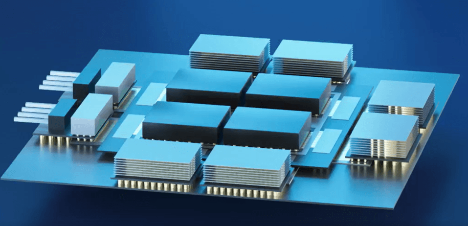
This article takes a peek inside one of those educational initiatives: a two-day hands-on training for imec’s pathfinding PDK (P-PDK) for the N2 node, the most advanced technology used in the industry today.
Participants from industry as well as academia were provided with the codes and files needed for digital design of N2 technology, and introduced to key concepts such as system-technology co-optimization (STCO), essential for further performance gains as traditional scaling slows down.
Published on:
28 June 2024