The NanoIC pilot line continues to grow its capabilities thanks to strong partner collaborations across Europe. One such partnership is with the Center for Surface Science and Nanotechnology (CSSNT) at the National University of Science and Technology Politehnica Bucharest (UPB).
Together they are strengthening the NanoIC pilot line’s ability to perform advanced metrology on complex 3D structures at the atomic level.
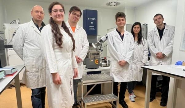
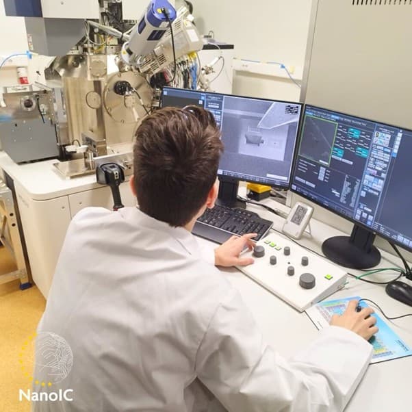
As part of the NanoIC pilot line project, CSSNT-UPB researchers recently completed a hands-on training at imec, gaining experience with advanced techniques such as lamella preparation, ion beam tool operation, and detailed inspection procedures used throughout semiconductor device fabrication.
This integration accelerates learning cycles and expands the pilot line’s capacity to support future prototyping and metrology requests.
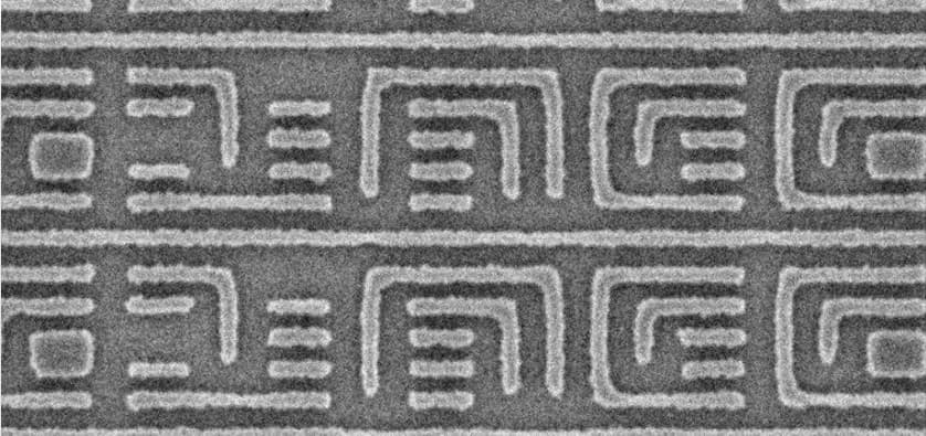
Metrology is a cornerstone of semiconductor manufacturing. Throughout the process, wafers are routinely paused for inspection. Thin cross-sections are prepared using FIB and analyzed via STEM/SEM to identify defects such as etch irregularities, layer deviations, or material interactions.
With the knowledge gained, the CSSNT-UPB team can now independently validate the performance of increasingly complex devices, an important step toward advancing European semiconductor R&D.
This collaboration not only strengthens the university’s expertise in semiconductor materials, but also expands the services it can offer to European partners.
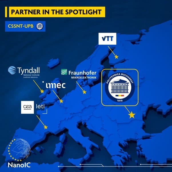
The NanoIC pilot line is a pan-European effort hosted by imec, in collaboration with CEA-Leti, Fraunhofer-Gesellschaft, VTT, Tyndall National Institute, and CSSNT-UPB. Together, we are building Europe’s most advanced semiconductor R&D and prototyping infrastructure for beyond-2nm technologies.
More partner updates will follow regularly.