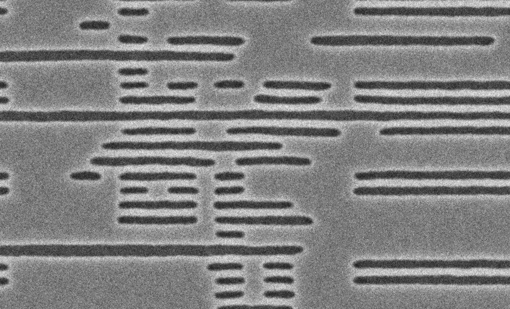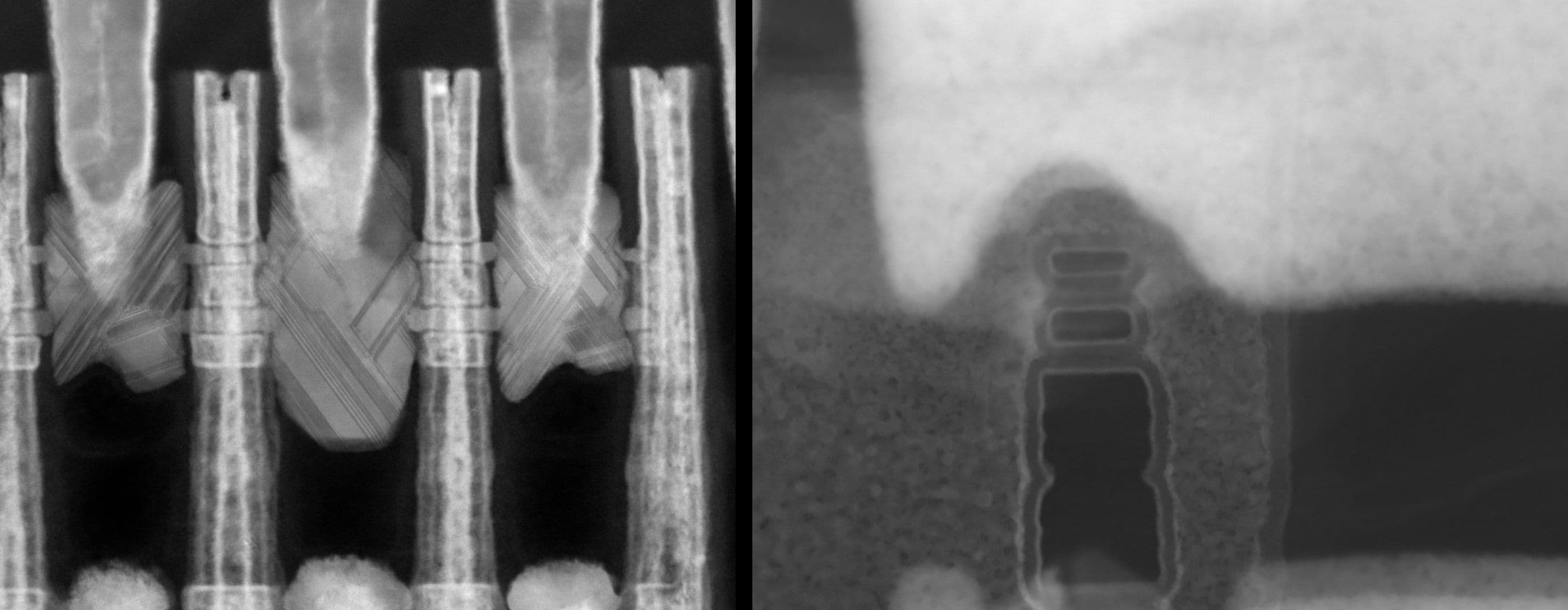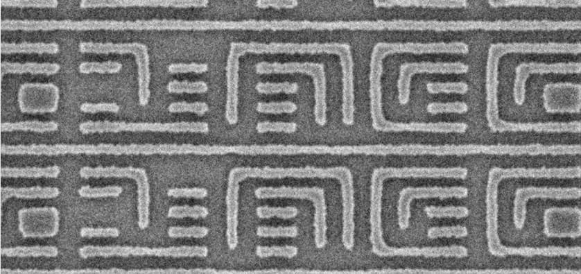

To accelerate innovation of beyond-2nm systems-on-chip, the imec-hosted NanoIC pilot line focuses on the development and maturation of selected advanced logic, memory, and interconnect technologies.
For logic, one of the key objectives is the development of a stable, manufacturable, and design-ready nanosheet platform, built around gate-all-around (GAA) nanosheet transistors.
To further secure Europe’s technological leadership, the NanoIC pilot line simultaneously works on developing the nanosheet’s successor: the complementary FET (CFET) – designed to extend the classical CMOS-based logic roadmap towards the A7 and beyond technology node. CFET is based on stacking n and pMOS transistors on top of each other, further shrinking logic standard cell sizes.
The CFET development flow involves the advancement and optimization of CFET-specific module processes and integration followed by device electrical validation, before eventually evolving towards baseline maturity and process design kit (PDK) development.
Critical CFET modules are the active device (built on a tall Si/SiGe epi stack), gate patterning and integration, junction formation and source/drain contact formation. While many of the GAA nanosheet process steps can be re-used, CFET module work is mainly being challenged by the verticality of the device structure, and the need for vertical isolation in critical parts of the stack cross-section.
In a new overview article – the first of a two-part article on CFET development – imec highlights progress in two CFET-specific process modules:
- an improved backside source/drain contact module,
- a gate-stack integration module that enables multiple threshold voltages in nanosheet and CFET devices.
The results were recently presented at the 2026 IEEE/JSAP Symposium on VLSI Technology & Circuits, the semiconductor industry’s premiere international conference integrating technology, circuits, and systems.
Published on:
8 September 2026