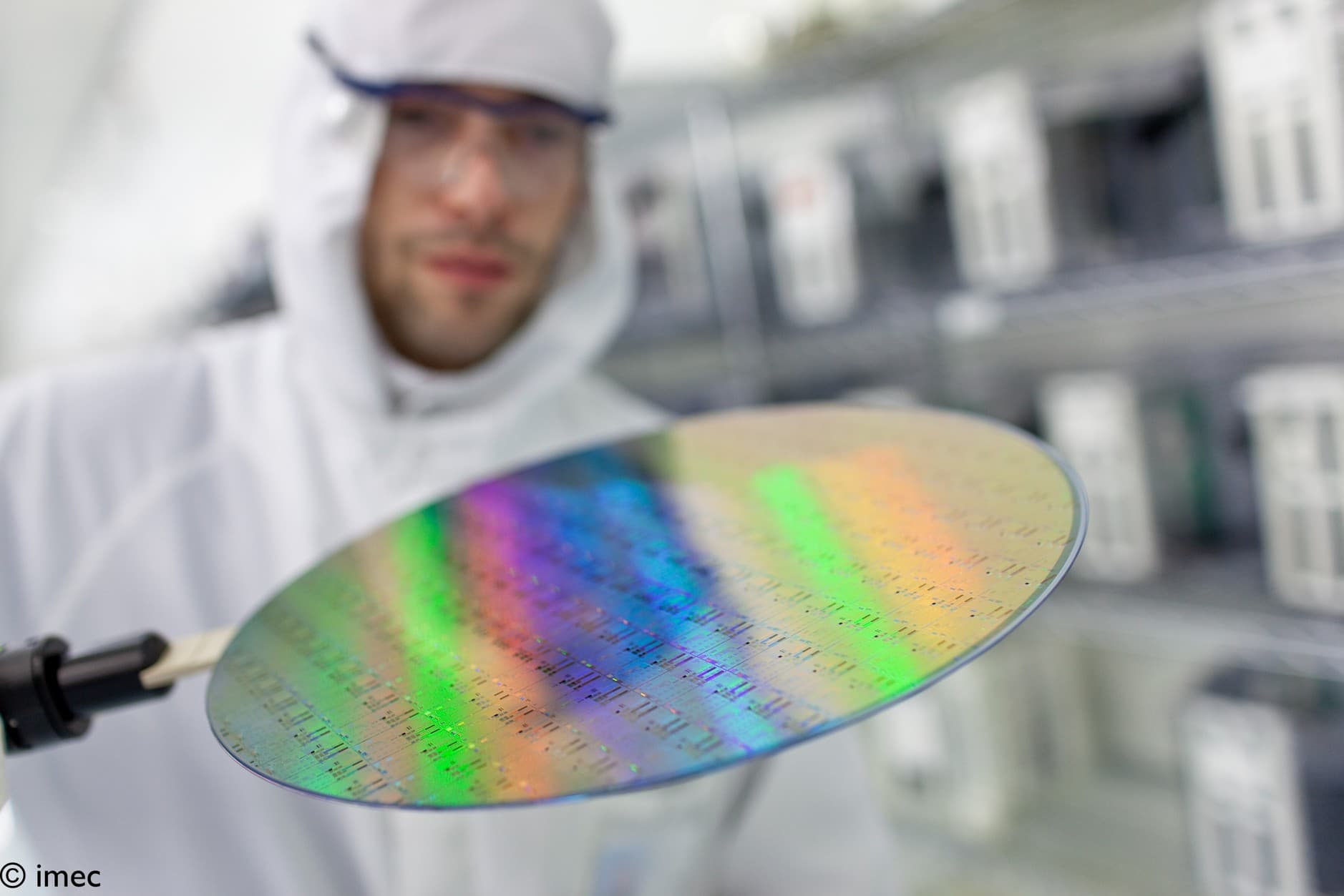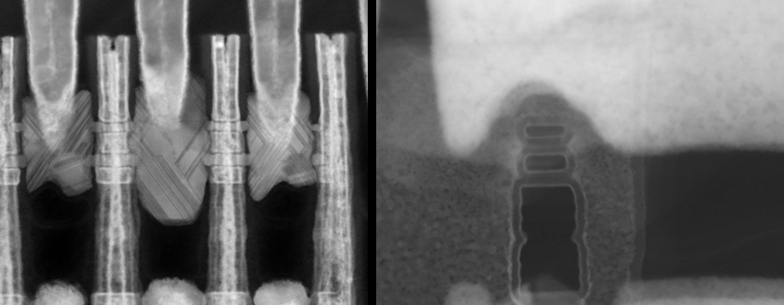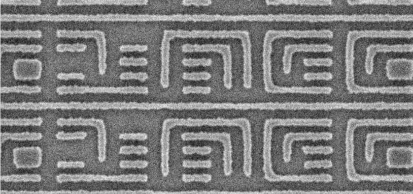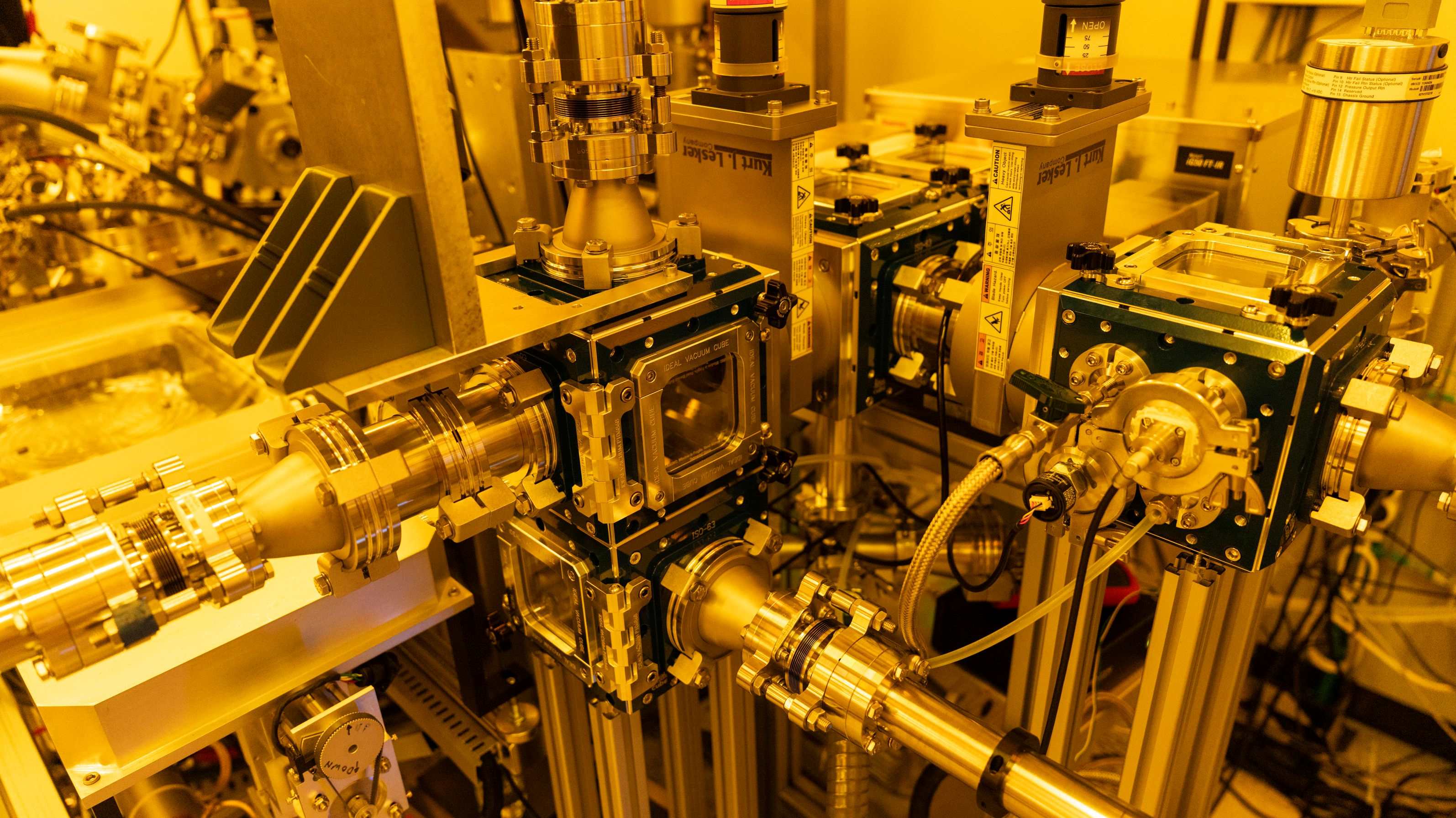
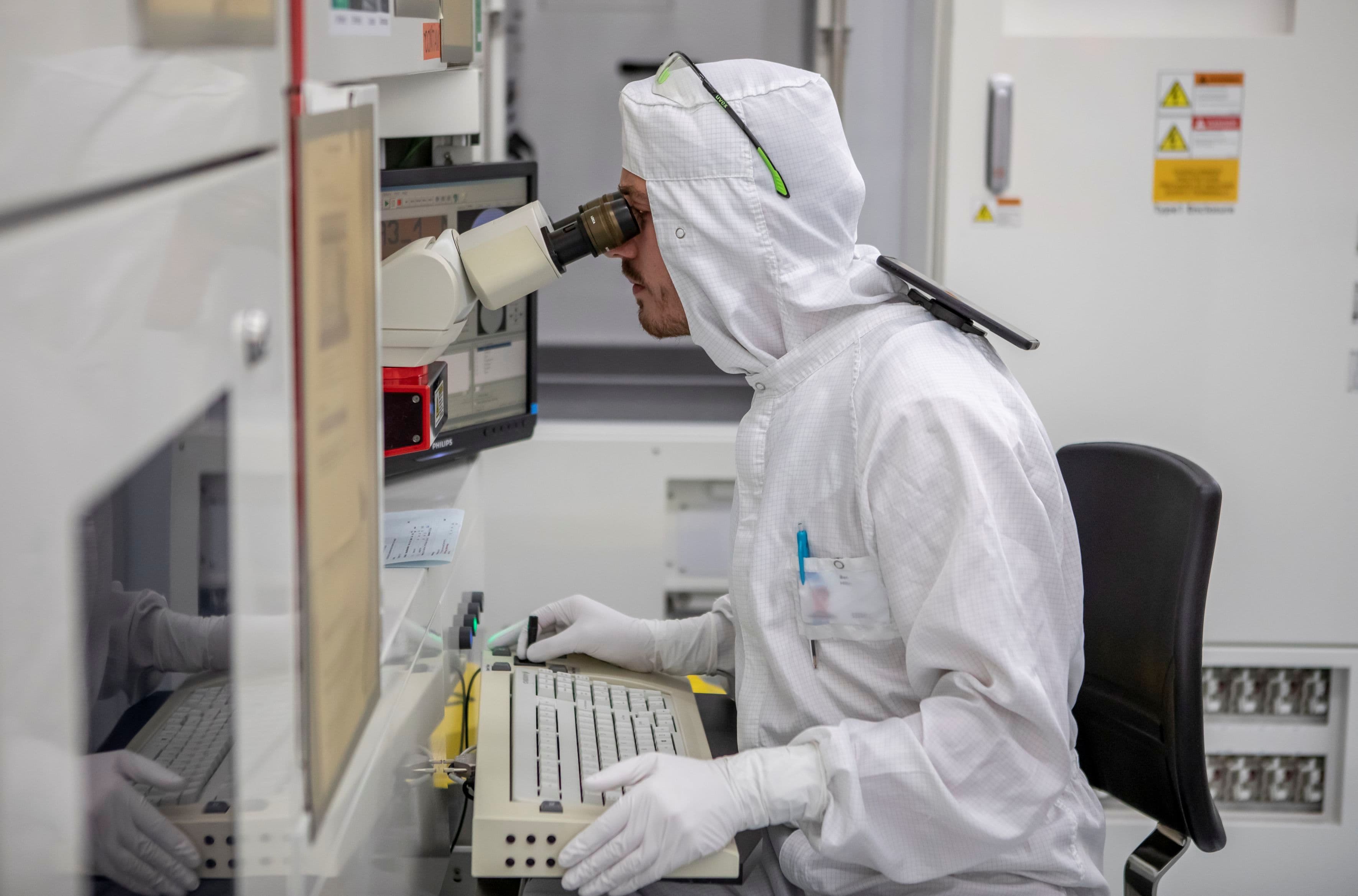

Metrology and inspection steps are critical for fast feedback to process development. They are extensively used in new process and module development and in monitoring the stability of baseline process flows.
As such, they are indispensable in developing beyond-2nm system-on-chip baseline flows for advanced logic, memory, and interconnects – which is a key objective of the NanoIC pilot line. The pilot line’s efforts focus on ensuring sufficient metrology capacity to improve learning speed, as well as on adding new metrology capability, tuned to the needs of advanced sub-2nm technology development.
A recently published overview article takes a closer look at the overall in-fab metrology and inspection toolbox, and how it evolved and diversified over the past four decades.
Driven by advances in lithography and patterning, as well as by innovations in device materials and architectures, new metrology and inspection techniques have emerged to complement optical methods – many pioneered by imec and its partners in metrology.
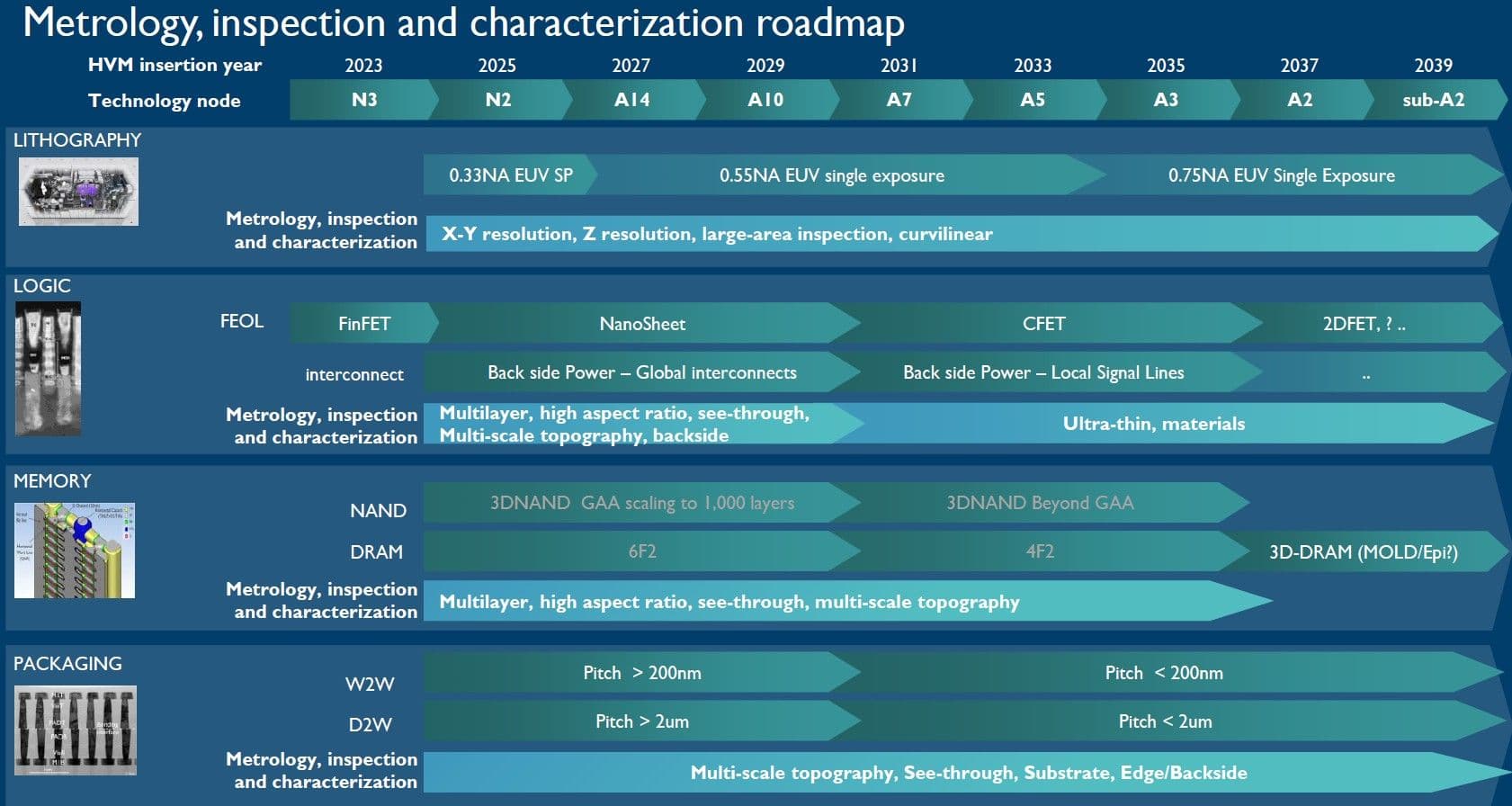
But the story doesn’t stop there. The next 40 years, metrology and inspection will be key in supporting continued dimensional scaling and the rise of 3D technologies, while meeting demands around cost and sustainability.