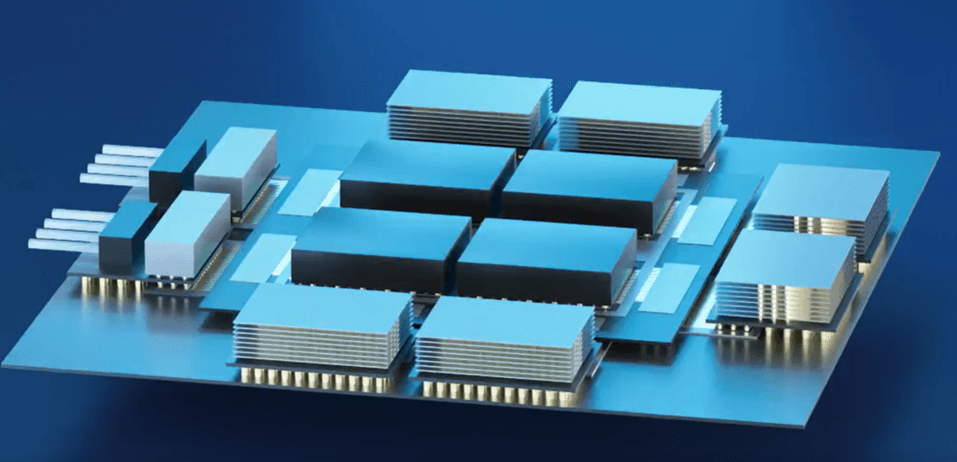
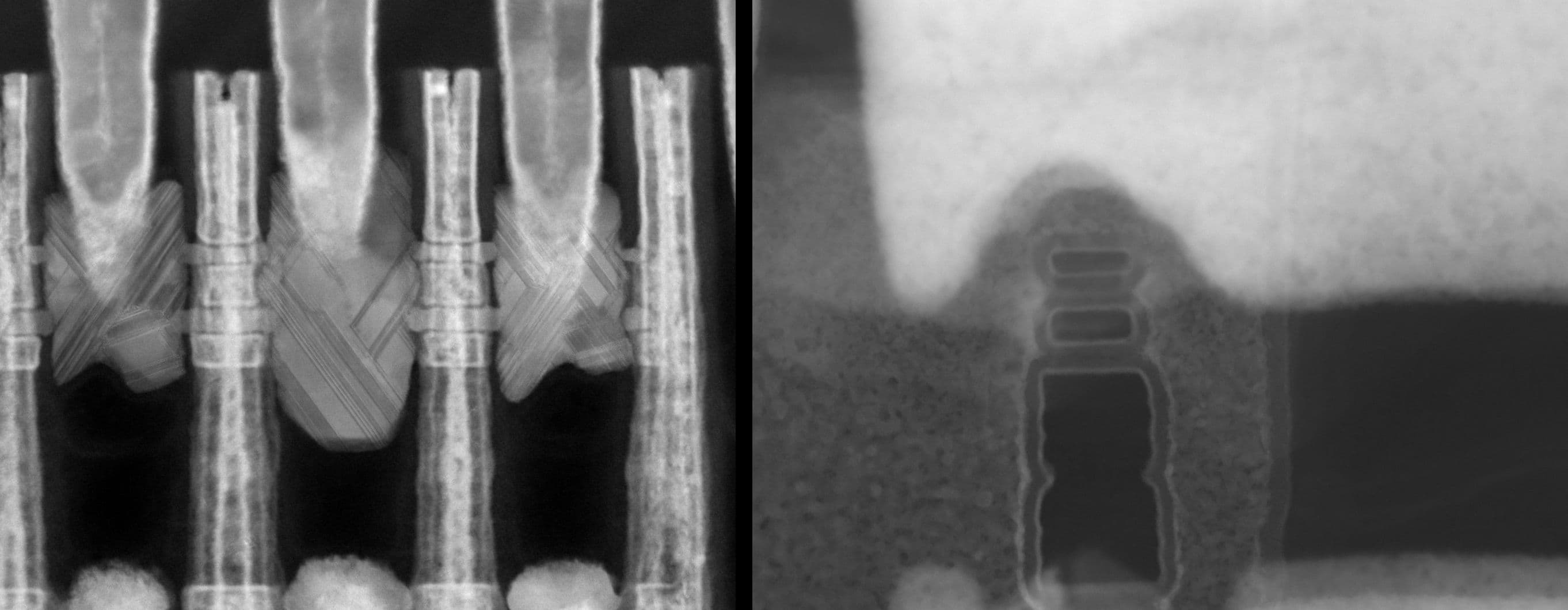
What will it take to turn CFET into a manufacturable technology for future logic nodes?
As the semiconductor industry moves towards the ångström era, complementary FET (CFET) architectures are emerging as an important option for extending the logic scaling roadmap.
Within the European NanoIC pilot line, CFET development is therefore one of the key enabling technologies being explored for beyond-2nm systems-on-chip.
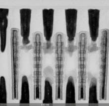
Recent imec research demonstrates further progress in this direction, combining advances in CFET integration with design-technology co-optimization (DTCO) studies.
The aim of these DTCO studies: to identify standard-cell configurations and performance boosters that offer the best trade-offs in power, performance and area across future technology nodes.
In part 2 of imec’s CFET roadmap article series, Geert Hellings shares unique insights into the latest DTCO results obtained by imec, including:
- A scalable sequential CFET architecture enabling split-gate devices
- New opportunities for extending both logic and SRAM scaling
- Approaches to improving back-end-of-line routability as CFET standard cells continue to scale
These results provide another step towards understanding what is needed to bring CFET technology towards future technology nodes.
Want to explore the results in more detail?
Read the full Advancing the CFET-based device roadmap article, part 2 on the imec website
Published on:
30 October 2026