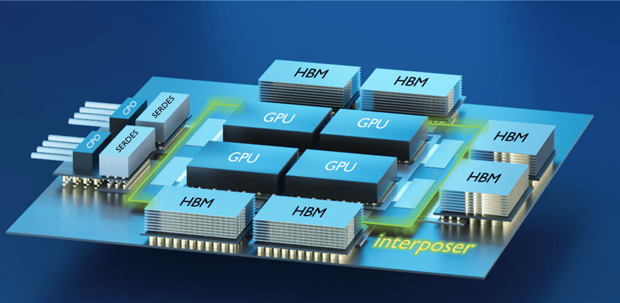

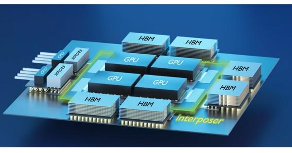
Every high-end AI accelerator or GPU shipping today pairs a compute die with several HBM (High Bandwidth Memory) stacks on a silicon interposer: a passive routing layer, patterned in silicon rather than a package substrate, reaching wiring densities substrates cannot match.
TSMC’s Chip-on-Wafer-on-Substrate (CoWoS) process, developed with Xilinx, produced the first commercial silicon interposer around 2011. For most of the decade that followed, it stayed a specialist choice for two- to four-die FPGAs and HPC parts.
Generative AI changed that. As ever larger AI models placed higher demands on memory bandwidth, moving data efficiently between compute and memory became a critical system-level challenge. Interposer manufacturing capacity soon became as strategic a bottleneck as leading-edge logic capacity itself.
At the same time, to reach higher levels of system performance, the semiconductor industry has been moving toward chiplet-based architectures, where multiple specialized dies were integrated into a single package. This shift dramatically increased the need for dense, high-bandwidth die-to-die communication, making silicon interposers one of the key technologies enabling this form of 2.5D integration.
Today, silicon interposers remain the default substrate for the highest-bandwidth multi-die systems, and the reference point everything else is measured against. They find their way into a growing range of applications, ranging from AI accelerators and GPUs to mmWave communication systems, co-packaged optics, aerospace, defense, and space systems.
Their designs are pushing toward reticle-size limits and eight to sixteen metal layers, with glass substrates and co-packaged optics emerging as the next steps once they reach volume production later this decade.
Yet access to advanced interposer technology typically remains restricted to a handful of large players through foundry NDAs. As a result, early design work is out of reach for much of Europe’s research and fabless community — until now.
Inside imec’s Si interposer
Imec’s Si interposer, developed within the NanoIC pilot line, is imec’s answer to that gap. At its core, the platform provides the dense vertical and horizontal interconnects needed to efficiently connect chiplets, memory and other specialized dies within a single package.
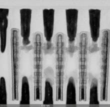
Signals move vertically through TSVs (through-silicon vias) etched into the silicon body, then fan out through five upscale copper-oxide BEOL interconnect layers. A frontside passivation stack, including an aluminum redistribution layer and under-bump metallurgy (UBM), terminates in frontside microbumps for die attach, while a backside polymer-based copper RDL and solder-ball pads close out the package on the substrate side.
The reference cross-section is shown in Figure 1; building it requires both frontside and backside processing.

Figure 1: Schematic representation of imec silicon interposer build-up
This five-layer, TSV-based build-up gives imec’s process the routing density used in today’s HBM-class 2.5D packages, while the frontside/backside flow keeps assembly compatible with the microbump and solder-ball processes already standard elsewhere in the industry.
Building it: frontside and backside processing
Si interposer processing starts with the TSV module and five metal layers to frontside passivation and microbumping, summarized in Figure 2. Backside processing then thins the wafer, reveals the TSVs, and builds the backside polymer RDL and solder-ball pads, finishing with temporary bonding to a second carrier and removal of the first — shown in Figure 3 — to free the interposer for top-die assembly.
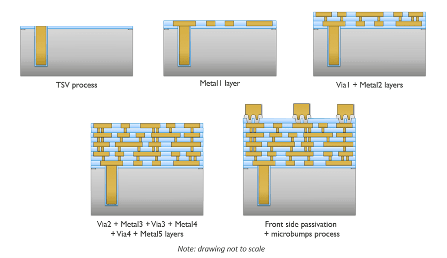
Figure 2: Reference flow for frontside processing of silicon interposer with 5 BEOL metal layers

Figure 3: Reference flow for backside processing of silicon interposer with 5 BEOL metal layers
The next missing link
As mentioned, access to advanced interposer technology remains largely restricted, limiting opportunities for researchers, start-ups and fabless companies to evaluate and develop next-generation heterogeneous systems.
That’s why imec is developing an advanced process design kit (PDK) for its silicon interposer technology within the NanoIC pilot line, giving researchers and companies a way to start exploring the technology before it fully matures.
Like imec’s pathfinding PDKs for advanced logic, the Si interposer PDK is built to give researchers a head start before the technology fully matures. A first release (V0), which will be available to eligible EU stakeholders, is targeted around early 2027, and will provide open, non-NDA design rules for the interposer platform within standard EDA environments such as Cadence and Synopsys.
The PDK will gradually mature from an initial design pathfinding release towards increasingly hardware-calibrated and silicon-validated versions, with upcoming releases planned for 2028.
Looking ahead, NanoIC's longer-term ambition is to extend this virtual exploration via a PDK into physical silicon demonstrators on the pilot line.
The ambition, as with imec’s pathfinding PDKs, is broader than one design kit: keeping the interconnect layer, that increasingly decides how our future AI hardware gets built, open to Europe’s research groups, start-ups, and fabless teams — as part of the same resilient, next-generation semiconductor ecosystem NanoIC is building across the pilot line.
Interested in further exploring NanoIC's interconnect PDKs?
NanoIC has already released a first version of two advanced interconnect PDKs: the fine-pitch redistribution layer (RDL) PDK and the die-to-wafer hybrid bonding (D2W) PDK. More information on available PDKs and access conditions can be found on the NanoIC PDK access page.
Updates of these PDKs, as well as the first release of the silicon interposer PDK will follow over the upcoming months. To receive updates on this PDK release and access opportunities, subscribe to the NanoIC mailing list.