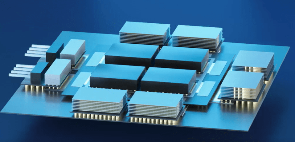
At the 2025 Symposium on VLSI Technology and Circuits (VLSI 2025), a unique world-class international conference where experts from industry and academia discuss state-of-the-art semiconductor innovations, imec will present several papers that highlight progress in advanced logic and memory technologies that are being developed in the framework of the NanoIC pilot line.
In one paper, imec presents a novel forksheet device architecture that allows to extend the nanosheet technology era to the logic A10 technology generation [1]. Other papers discuss improvements to imec’s process flow for monolithic CFET devices, which are expected to succeed nanosheet and forksheet architectures from the A7 node onwards. Improvements are reported for several critical process modules, including source-drain junctions, device contacts, and gate stacks [2,3]. Also highlighted are the scaling opportunities that advanced CFET architectures can provide to SRAM memory bit cells. [4]
In compute system architectures, 2nm and beyond logic technologies may be implemented in combination with a backside power delivery network – an innovative way of delivering power to the transistors by moving the power distribution network to the wafer’s backside. At 2025 VLSI, imec discusses the benefits that such a backside power delivery scheme may bring for a 2nm mobile computing processor, in always-on as well as in switched-power designs [5].

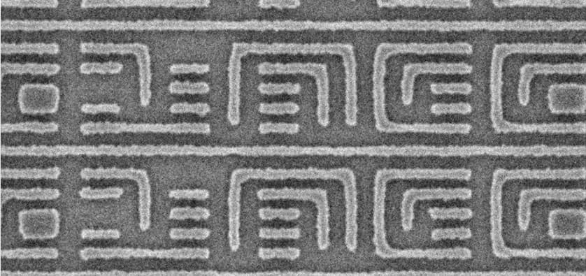
Transmission electron microscopy (TEM) image of monolithic CFET devices
In the field of memory, a novel integration flow for 3D DRAM is presented, which can serve as a baseline for more fundamental device research [6]. 3D memories including 3D DRAM and other non-volatile memories will become important to achieve high density memories to address the memory wall challenge especially for AI inference and training. A generic 3D memory platform is one of the enablers in the NanoIC project.
Finally, imec reports optimization of its STT-MRAM architecture and process flow resulting in density and performance gains over previous designs. The presented processing approach can potentially be used to improve SOT-MRAM as well, a memory technology that is being developed in the framework of NanoIC as a promising dense embedded memory concept. [7]
Overview of the imec 2025 VLSI papers relevant to the NanoIC pilot line
[1] ‘Extending the gate-all-around (GAA) era to the A10 node: outer wall forksheet enabling full channel strain and superior gate control,’ L. Verschueren et al.
[2] ‘Monolithic CFET flow improvements integrating cover spacer and dual-WF RMG,’ C. Cavalcante et al.
[3] ‘Shifter materials and stack explorations for Vt fine-tunable dual dipole multi-Vt gate stacks compatible with low thermal budget CFET,’ H. Arimura et al.
[4] ‘SRAM scaling opportunities below 0.01 μm² using double-row CFET architecture with wordline-folded bitcell design for performance optimization,’ D. Abdi et al.
[5] ‘Backside power delivery for power switched designs in 2nm CMOS: IR drop and block-level power-performance-area benefits,’ Y. Zhou et al.
[6] ‘Process Insights into 3D-DRAM with vertical bit line and scalable GAA transistor,’ N. Rassoul et al.
[7] ‘High density, high speed STT-MRAM N7 macros: materials and DTCO exploration,’ D. Narducci et al.