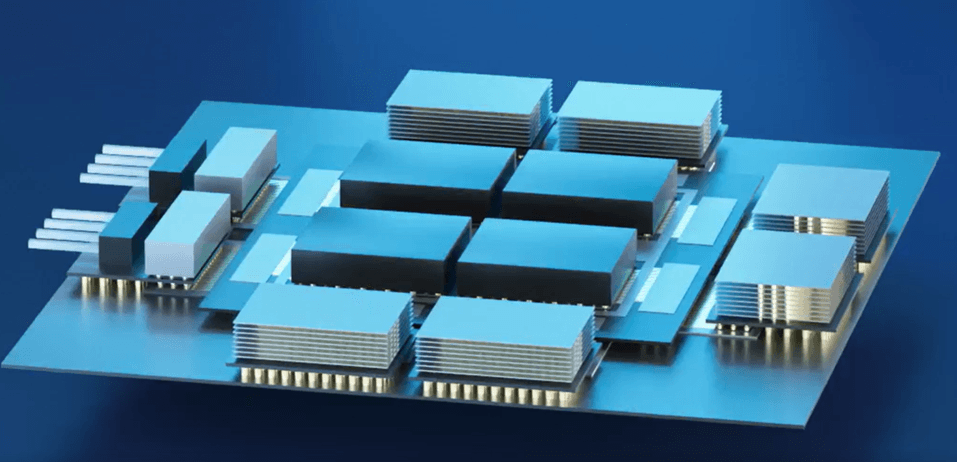
Outer wall forksheet: a scalable bridge from nanosheet to CFET for next-gen logic
As the semiconductor industry advances toward the 2nm technology node and beyond, the need for innovative device architectures becomes increasingly urgent. The outer wall forksheet, pioneered by imec and enabled by NanoIC, represents a critical step in this evolution—offering a manufacturable, high-performance successor to traditional nanosheet FETs before the complementary FET (CFET) enters the roadmap.
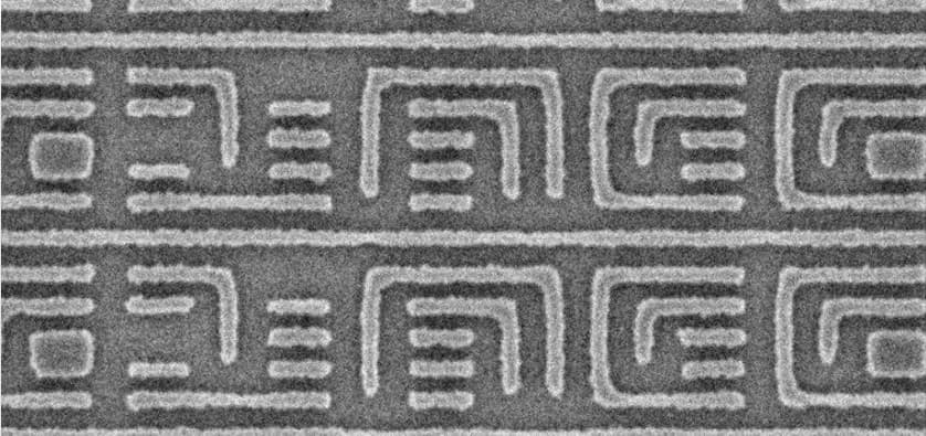
Unlike inner wall forksheet designs, the outer wall approach simplifies fabrication by placing the dielectric wall at the standard cell boundary and by fabricating the wall using a wall-last integration approach. This architecture not only enhances short-channel performance but also supports vertical stacking, allowing to extend the logic technology roadmap to the A10 technology node.
Discover how this breakthrough supports the NanoIC project's mission to accelerate beyond-2nm logic technologies while aligning with Europe's strategic semiconductor roadmap.
This article was originally published in EE Times.
Published on:
12 June 2025