The full article can be found in Markt&Technik (German only)
The NanoIC pilot line is a strategic initiative under the EU Chips Act aimed at advancing Europe's leadership in next-generation semiconductor technologies.
As emphasized by Henna Virkkunen and other leaders at ITF World 2025, Europe's semiconductor future depends on collective action. Industry stakeholders, researchers, policymakers, and investors are encouraged to actively contribute to shaping the next phase of the Chips Act and to engage with the NanoIC initiative. This is a unique opportunity to help build a resilient, innovative, and globally competitive semiconductor ecosystem in Europe.
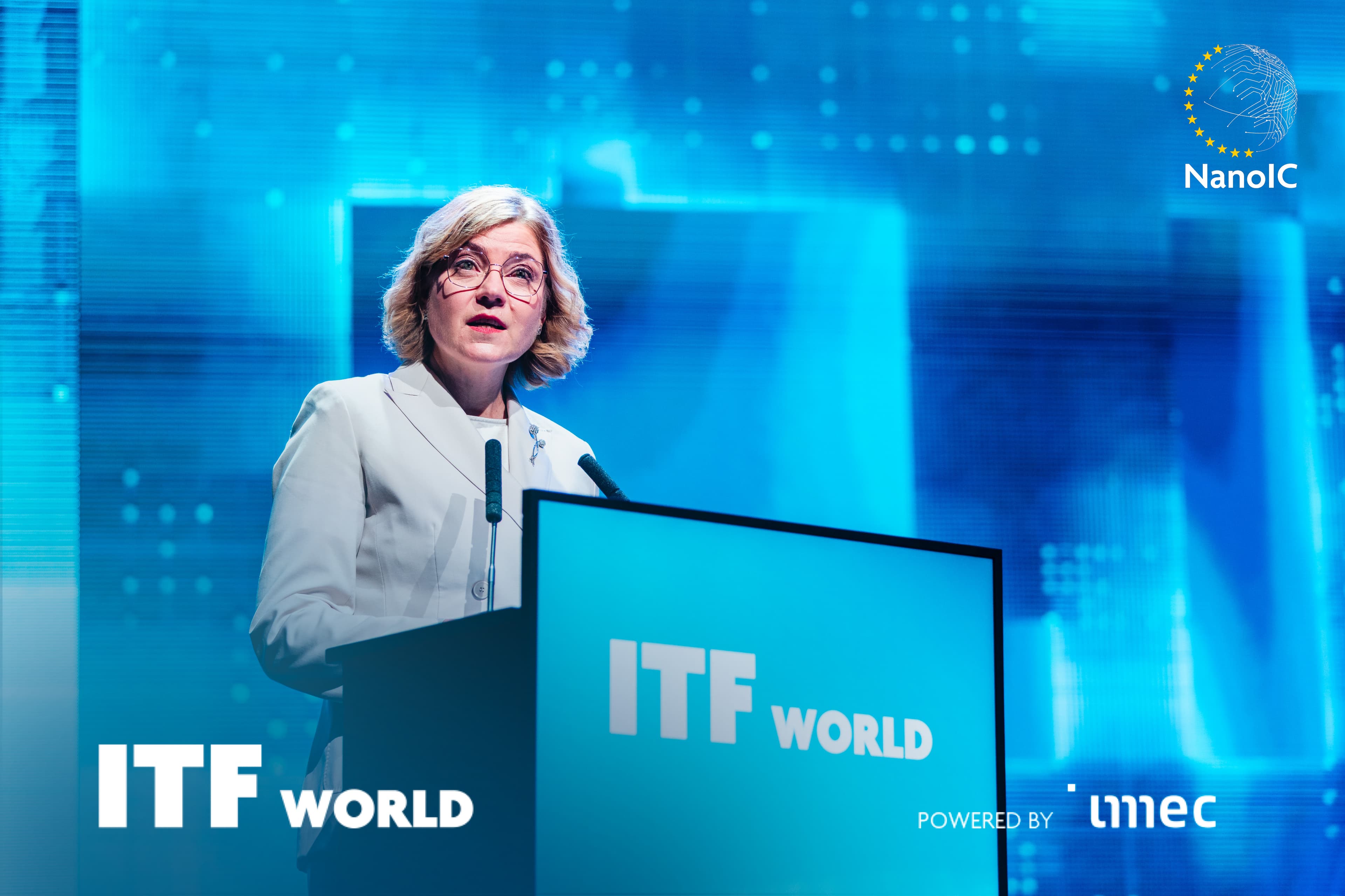
Henna Virkkunen, Executive Vice-President of the European Commission for Technological Sovereignty, Security, and Democracy, at ITF World in Antwerp, Belgium (May, 2025).
What the article highlights:
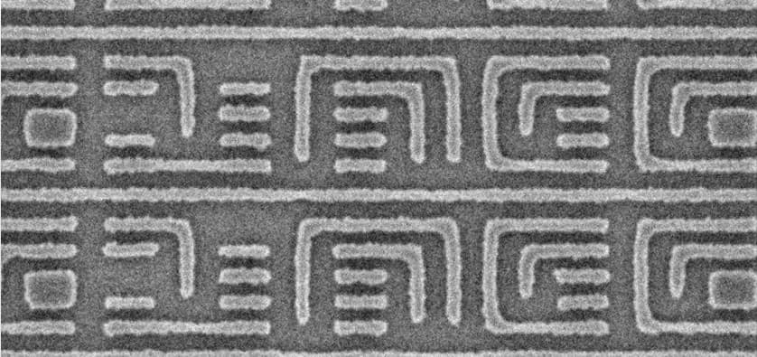
- NanoIC’s mission to accelerate the development of advanced semiconductor technologies in Europe, including nanosheet transistors, CFETs, 3D interconnects, and embedded memory such as SOT-MRAM and eDRAM.
- The 300-mm pilot line in Leuven, Belgium, is designed to serve startups, SMEs, and academia, bridging the gap between research and scalable manufacturing. The open access model ensures a shared infrastructure for research, prototyping, and training.
- The integration of SmartFab concepts like digital twins and AI-driven process control to shorten learning cycles and increase transparency.
- Training and upskilling are embedded in the project, ensuring a new generation of semiconductor talent in Europe.
- NanoIC’s role in strengthening Europe’s technological sovereignty and reducing reliance on non-European fabs.
Read the full article "NanoIC-Pilotlinie: Europas strategischer Sprung in der Halbleiterinnovation“ on pages 14-19